
Scaling Up Metasurfaces: Accuracy, Computational Cost, and Artificial Intelligence
News originally published by
EIN Presswire
These include unit-cell methods based on local periodic responses, coupling-aware modeling, adaptive spatial sampling, and multifunctional meta-atoms; supercell methods for intracell coupling and diffraction-order control; and full-metasurface methods us

Each segment is characterized by its initial wrapped phase and unwrapped phase excursion. (a) Reuse ratio and normalized cumulative width of representative segments versus segment width. (b) Reuse ratio versus the similarity threshold for three lens radii
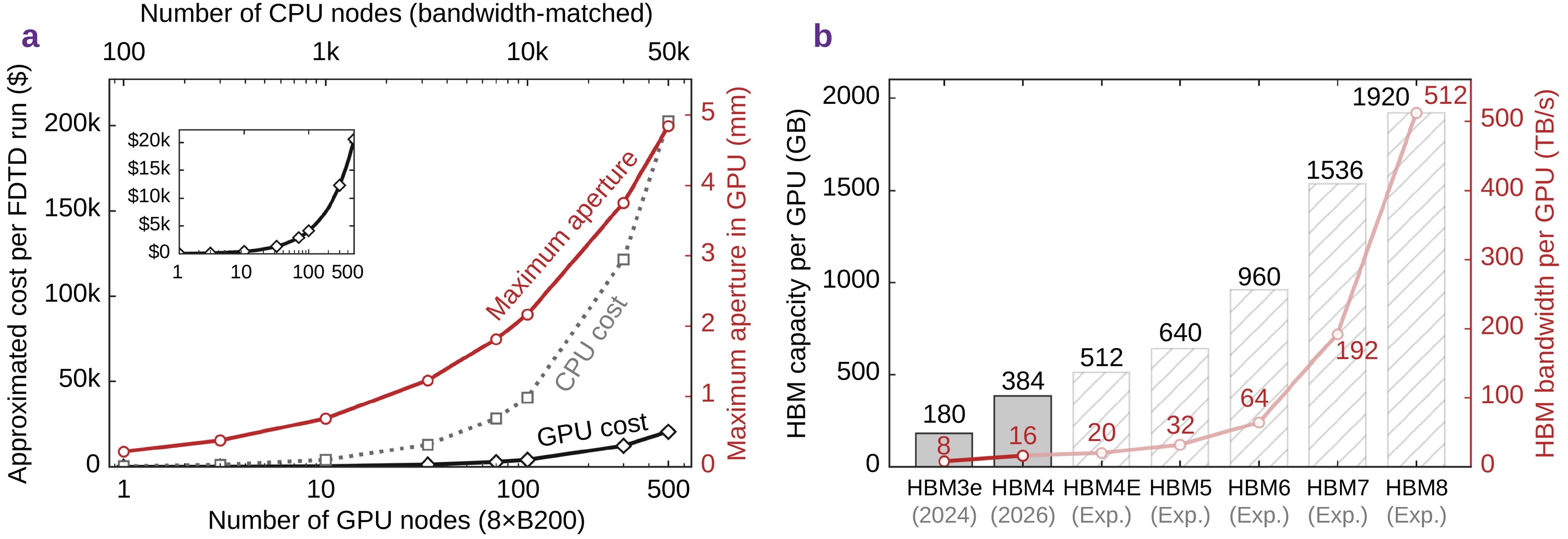
(a) Estimated cost of a single FDTD solve and the ideal memory-capacity-based aperture limit versus the number of eight-GPU nodes, with a nominal bandwidth-matched CPU comparison. (b) High-bandwidth memory (HBM) capacity and bandwidth for a reference GPU
A review examines metasurface design across scales, connecting reusable building blocks, full-aperture inverse design, and artificial intelligence
SICHUAN, CHINA, November 6, 2026 /EINPresswire.com/ -- Large-area metasurface design requires a balance between electromagnetic accuracy, response reuse, and computational cost. Researchers at Hanyang University and Korea University review unit-cell, supercell, and full-metasurface approaches, together with neural-network-assisted simulation and inverse design. Analyses of radial phase-segment reuse and finite-difference time-domain resource requirements quantify distinct aspects of design scalability. The review discusses the assumptions, fabrication constraints, and validation requirements that determine the applicability of each method for large-aperture optical devices and systems.Metasurfaces control the phase, amplitude, and polarization of light using subwavelength structures arranged within a thin optical layer. Spatially varying responses enable beam steering, focusing, holography, and compact imaging. Extending these functions to large apertures requires design methods that account for the optical response of the complete device without an excessive computational cost.
Conventional unit-cell design constructs a library of meta-atom responses calculated under periodic boundary conditions. These responses are assigned across the aperture to approximate a prescribed optical profile. The local periodic approximation assumes that each meta-atom retains the response obtained from an array of identical elements. Reusing a finite library avoids repeated full-wave optimization of the entire device and makes large-area design computationally tractable.
The approximation becomes less accurate when dissimilar neighboring elements alter the local electromagnetic response. Finite spatial sampling can also limit the representation of steep phase gradients, while broadband and multifunctional operation require increasingly complex wavelength-, polarization-, and angle-dependent responses. These limitations depend on the target field, material platform, and local geometry; aperture size alone does not determine whether a local description is adequate.
Inverse design optimizes a structure for a specified optical objective. It can be applied to individual unit cells, interacting groups of elements, or the complete aperture. Enlarging the jointly treated region allows electromagnetic interactions within that region to influence the optimization, but increases the cost of repeated field calculations. Full-aperture calculations are particularly demanding for three-dimensional devices at visible wavelengths.
The choice of design method therefore depends on the required accuracy, interaction range, achievable response reuse, and available computational resources. Comparing these methods requires attention to the assumptions of each electromagnetic model, its numerical implementation, and the fabrication constraints imposed on the resulting structure.
The research groups of Prof. Haejun Chung at Hanyang University and Prof. Sunae So at Korea University review these large-area metasurface design strategies in “Scaling Metasurface Design: From Reusable Unit Cells to Full-Metasurface Inverse Design.” The review organizes design strategies by the electromagnetic domain treated jointly and examines neural-network-based methods across these spatial scales. It is made available online on October 25, 2026, and published in Volume 5, Issue 10 of the journal Opto-Electronic Science.
For unit-cell design, the review examines spatial sampling, intercell coupling, and the expansion of local optical responses for multifunctional operation. Adaptive sampling and alternative lattice arrangements can improve the representation of target fields. Coupling-aware models include neighboring geometries in response prediction, while dispersion and polarization engineering extend the functions available within a library-based approach.
Periodic supercells treat several interacting elements as a composite unit and control the complex amplitudes of available diffraction orders. Section-wise and overlapping-domain approaches instead enlarge the local simulation region without necessarily introducing a repeated physical supercell. These methods include a wider range of interactions, although coupling between separately treated regions can produce stitching errors.
The authors also analyze reuse of reduced radial phase patterns in an ideal axisymmetric metalens. Under the stated conditions, the reuse ratio decreases from 71.4% to 3.0% as the segment width increases from one to six wavelengths, indicating that broader segments are less likely to recur. This metric describes similarity in phase representation, not electromagnetic equivalence, optical performance, or computational savings.
Full-metasurface inverse design treats the entire aperture as a coupled electromagnetic system, allowing device-level performance, such as focusing efficiency and imaging quality, to be optimized while accounting for interactions across the structure. By including interactions beyond local models, this approach improves physical accuracy but requires substantially higher computational resources. A hardware-aware FDTD analysis estimates this scaling challenge: under the specified assumptions, a one-centimeter square aperture requires approximately 3.1 petabytes of resident memory. These estimates describe individual electromagnetic calculations rather than complete inverse-design optimization.
Neural-network-based methods provide response and field surrogates, candidate-generation models, and learned components within iterative solvers. Physics-informed learning and neural operators are examined alongside tandem and generative inverse-design networks. Their computational benefit depends on data-generation and training costs, repeated use, and prediction accuracy within the validated domain.
Active learning and transfer learning can reduce the need for new labeled data, while minimum-feature constraints and process models account for fabrication. End-to-end approaches optimize optical and computational components against system-level objectives; image restoration for a fixed fabricated optic is distinguished from joint optimization. The review also discusses model interpretation and accessible design tools. Final structures require full-wave verification, and experimental results must be assessed under the relevant fabrication and operating conditions.
Further development requires coupling-aware local models, adaptive overlapping domains, and distributed full-wave solvers with lower memory requirements. Neural operators can assist repeated field calculations, provided that predicted fields and design gradients are validated against reference simulations. Fabrication models and optical measurements should be incorporated into subsequent optimization to reduce discrepancies between simulated and measured performance. Reconfigurable metasurfaces introduce additional control variables that can be optimized jointly with the passive geometry. Consistent reporting of simulation dimensionality, numerical accuracy, memory, runtime, fabrication constraints, and experimental performance would support comparisons of design methods under clearly defined conditions.
Reference
Title of original paper: Scaling metasurface design: from reusable unit cells to full-metasurface inverse design
Journal: Opto-Electronic Science
DOI: https://doi.org/10.29026/oes.2026.260058
About Opto-Electronic Science
Opto-Electronic Science (OES) is a premier, open-access, peer-reviewed journal boasting an impressive Impact Factor and CiteScore. Indexed in major databases like Scopus, ESCI, DOAJ, and CA, OES serves as a leading platform for academic exchange and innovation in optics and optoelectronics. The journal publishes high-impact articles, reviews, and letters spanning diverse fields—such as quantum optics, ultrafast optics, micro/nano-optics, biophotonics, and integrated optics. Headquartered in Chengdu, China, OES bridges fundamental scientific breakthroughs with cutting-edge technological advancements in the global research community.
Website: https://www.oejournal.org/oes/
About the Research team of Prof. Haejun Chung at Hanyang University
The Computational Photonics and AI Design Lab at Hanyang University, led by Prof. Haejun Chung, develops optical and electromagnetic devices through large-scale simulation, inverse design, and artificial intelligence. Its methods include adjoint optimization, physics-guided neural operators, and diffusion-based generative models. Research topics span metasurfaces, visible and thermal-imaging metalenses, CMOS image-sensor color routers, augmented-reality waveguide couplers, integrated photonics, and quantum optics. The group also co-designs optical hardware and image-reconstruction algorithms for compact imaging and under-display cameras. Through academic and industrial collaborations, the lab connects computational advances with practical device development. Its metalens-imaging research received two CES 2025 Innovation Awards and was selected among Korea’s Top 100 National R&D Achievements.
About the Research team of Prof. Sunae So at Korea University Sejong Campus
The Smart Optics Lab at Korea University Sejong Campus, led by Prof. Sunae So in the Department of Electro-Mechanical Systems Engineering, studies nanophotonics and AI-assisted inverse design. Its research covers metasurface holography, augmented-reality optics, medical visualization, radiative cooling, and surface-enhanced Raman scattering sensing. The group combines FDTD and rigorous coupled-wave analysis, deep-learning surrogates, and adjoint-based topology optimization with fabrication constraints. Current projects include depth-aware holographic optics for medical visualization and waveguide optics for augmented-reality glasses. Supported by national and industry-sponsored projects, the group collaborates with POSTECH, KAIST, and the Korea Institute of Machinery and Materials on computational design, nanofabrication, and device integration.
Funding information
This work was supported by the National Research Foundation of Korea funded by MSIT (RS-2024-00338048, RS-2026-25487796, RS-2026-25620621, NRF-2022R1C1C2009430), and by the Ministry of Education (RS-2026-25571231), the Culture, Sports and Tourism R&D Program through KOCCA funded by MCST (RS-2024-00332210), IITP funded by MSIT (RS-2025-02283217, RS-2026-25507992), and the Alchemist Project funded by the Ministry of Trade, Industry and Energy (MOTIE), Republic of Korea, through the Korea Evaluation Institute of Industrial Technology (KEIT) (Project Nos. 1415179744 and 20019169).
Siyi Ma
Institute of Optics and Electronics, Chinese Academy of Scie
+86 19136186296
oej_publishing@ioe.ac.cn
Legal Disclaimer:
EIN Presswire provides this news content "as is" without warranty of any kind. We do not accept any responsibility or liability for the accuracy, content, images, videos, licenses, completeness, legality, or reliability of the information contained in this article. If you have any complaints or copyright issues related to this article, kindly contact the author above.
